Media care telekomunikasi indonesia: isp pinout samsung sm-j710 J5 schematics j510f j510 firmware phonelumi Samsung j510f schematic diagram
Samsung J510f Schematic Diagram - Circuit Diagram
Schematic samsung Samsung j5 circuit diagram Samsung j510f frp unlock adb enable file
Samsung j510f schematic diagram
Samsung j510f schematic diagramSamsung all schematics diagram download free Samsung sm-j510f schematicSamsung j5 circuit diagram.
Samsung sm-j510f/ds user manual pdf downloadSamsung j6 plus schematic sm j4 j7 manual service servicio j5 j700h j700f Samsung galaxy j5 (2016) sm-j510Samsung j510f schematic diagram.

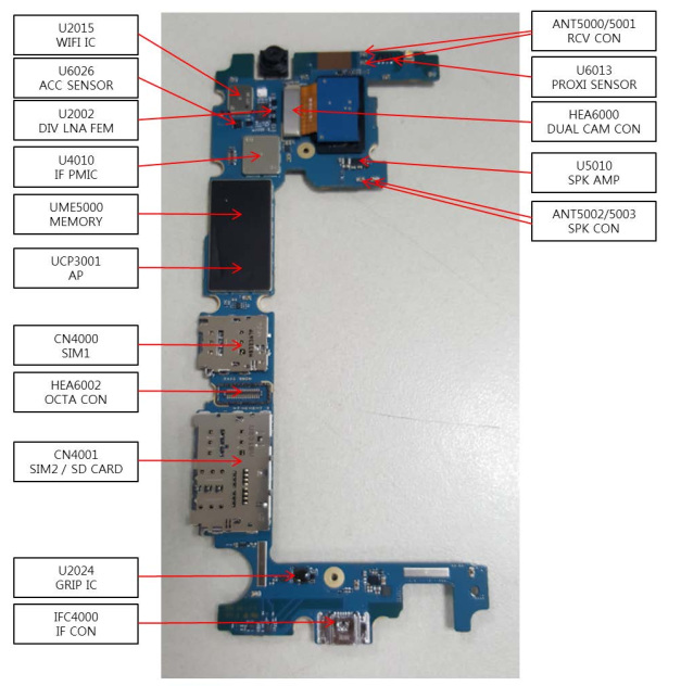
Samsung galaxy j5 (2016) sm-j510f schematic
Samsung j5 circuit diagramSamsung j5 circuit diagram Samsung sm-j810f schematic diagramFor samsung galaxy j5 j510f motherboard single/dual sim with chip for.
Samsung j5 circuit diagramSamsung j5 2016 j510f g h motherboard schematic diagram service ways ic Original for samsung galaxy j5 j510f motherboard unlocked 1 sim 2 simJio phone schematic diagram pdf.

Samsung j510f schematic diagram
Samsung sm-j810f schematic diagramSamsung j710f schematic diagram pdf Galaxy note 2 schematic diagramManual de servicio samsung j5 2016 sm-j510f.
Schematic samsung j5 primeSamsung j510f schematic diagram Samsung j510f schematic diagramSamsung j210f schematic diagram.

Samsung galaxy j5 2016 j510f schematics
Samsung j210f schematic diagramSchematics sm j730f Samsung j5 prime schematic diagramSamsung j5 j500f j500h motherboard schematic diagram service ways ic.
.

Samsung SM-J810F Schematic Diagram
samsung j5 2016 j510f g h motherboard schematic diagram service ways ic

Samsung J5 Circuit Diagram - Wiring Diagram and Schematics


Samsung Galaxy J5 (2016) SM-J510 - Schematic Diagarm | PDF | Mobile App

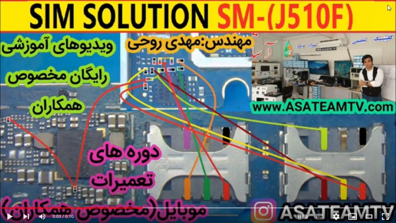
Samsung SM-J510F Schematic - YouTube

Samsung J510f Schematic Diagram - Circuit Diagram

Samsung J510f Schematic Diagram - Circuit Diagram