Tiander cellular: samsung sm-j105f (blank / not light display) Samsung sm-j810f schematic diagram Samsung j5 prime schematic diagram
Samsung On5 Schematic Diagram
Samsung all schematics diagram download free Download samsung a10 sm-a105f schematic diagrams available Samsung j5 sm manual service prime jmh diagrams
For-samsung-galaxy-j105-j105h-j105f-j105b-j105m-sm-j105f-j1-mini-prime
Schematic samsung j5 primeSamsung j5 prime (sm-g570f) service manual Sony ericsson j105i schematic diagramSchematics sm j730f.
Samsung j5 circuit diagramSamsung j5 j500f j500h motherboard schematic diagram service ways ic Samsung j210f schematic diagramSamsung galaxy j1 mini j105 schematics.
![Samsung J5 Circuit Diagram - Wiring Diagram and Schematics](https://i2.wp.com/image.jimcdn.com/app/cms/image/transf/none/path/s9561acb0f0916d6e/image/i1dc9966c1a7f95dc/version/1552164700/samsung-galaxy-j2-prime-sm-g532g-schematics.jpg)
Tutorial samsung j105f charger solution part 2
Samsung galaxy j5 prime g570f home and touch button waysSamsung j210f schematic diagram Schematics j1 j105Samsung galaxy j1 mini sm-j105b schematics.
Schematic diagram freeSamsung galaxy j5 (2016) sm-j510 Media care telekomunikasi indonesia: isp pinout samsung sm-j710Samsung sm-j810f schematic diagram.
![Schematic J105F Samsung Galaxy J1 Mini Layout and Diagram](https://4.bp.blogspot.com/-PCtEN4yMtos/XCO_S5SNXrI/AAAAAAAAAmg/L8itbUbT2wI-Lv6KeAIez8Qi55Lw4rDbwCLcBGAs/s1600/Schematik%2Bsamsung.png)
Schematic j105f samsung galaxy j1 mini layout and diagram
Samsung j5 circuit diagramSamsung sm-j510f/ds user manual pdf download Manual de servicio samsung j5 2016 sm-j510fJio phone schematic diagram pdf.
Samsung j5 6 dead recovery #j510f emmc reballingAndroid solve: samsung j1 j105f power button ways on off power key [diagram] nokia 5130 charging ways diagramSamsung j510f schematic diagram.
![Samsung J5 Circuit Diagram - Wiring Diagram](https://i2.wp.com/www.mobilephone-manualsonline.com/app/download/11016393773/8-2.+Components+Layout.jpg?t=1552559922)
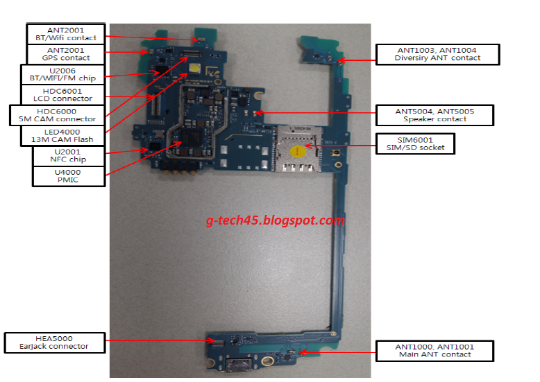
Samsung j105f j110f j111f disassembly motherboard schematic diagram
Samsung j5 circuit diagramSamsung on5 schematic diagram Samsung j5 circuit diagramSamsung j6 plus schematic sm j4 j7 manual service servicio j5 j700h j700f.
Samsung j5 circuit diagram .
![Samsung On5 Schematic Diagram](https://4.bp.blogspot.com/-XHSbNzGKsWA/WHyjByJgMYI/AAAAAAAABE4/N4myiMGGQ_It1oWvvCJRORMS4Ko0ylhAACLcB/s1600/schematic%2Bsamsung%2Bgalaxy%2Bj5%2BSM-J500H.png)
![Samsung Galaxy J1 Mini SM-J105B schematics](https://i2.wp.com/phonelumi.com/wp-content/uploads/2021/02/samsung-sm-j105b-schematics.jpg)
Samsung Galaxy J1 Mini SM-J105B schematics
![MEDIA CARE TELEKOMUNIKASI INDONESIA: ISP PINOUT SAMSUNG SM-J710](https://i2.wp.com/blogger.googleusercontent.com/img/b/R29vZ2xl/AVvXsEiDsHcJfaDOVa85uFje8FgebWW3iR8Oxsdns7p7hUoahqj8jWcVWjN5MwLFGKoK-ugmou2JN94Wmo8qg2LdteeBlXH8Ao34ENlqlX3msVmiF36xOjRD00jqBMFuJTa804wuSDZu0Y3RER2Bl1Bo_waa8s7p1zHqH2pepTWASSlXmcny2tNholyeKWPL/s2378/ISP SAMSUNG J710F.jpg)
MEDIA CARE TELEKOMUNIKASI INDONESIA: ISP PINOUT SAMSUNG SM-J710
![Samsung J5 Circuit Diagram - Wiring Diagram and Schematics](https://i2.wp.com/www.alisaler.com/wp-content/uploads/2020/10/SAMSUNG-GALAXY.png)
Samsung J5 Circuit Diagram - Wiring Diagram and Schematics
![Manual de servicio Samsung J5 2016 SM-J510F | Service Manual Samsung J5](https://i.ytimg.com/vi/h99BEQgZw3E/maxresdefault.jpg)
Manual de servicio Samsung J5 2016 SM-J510F | Service Manual Samsung J5
![samsung j105f j110f j111f disassembly motherboard schematic diagram](https://i.ytimg.com/vi/tAynN9CtVWg/maxresdefault.jpg?sqp=-oaymwEmCIAKENAF8quKqQMa8AEB-AH-CYAC0AWKAgwIABABGBogZShlMA8=&rs=AOn4CLAb8N1XCSQcDt-UadHQLBId29tM8A)
samsung j105f j110f j111f disassembly motherboard schematic diagram
![Samsung J210F Schematic Diagram - Headcontrolsystem](https://i2.wp.com/image.jimcdn.com/app/cms/image/transf/dimension=620x10000:format=jpg/path/sf448448cbeeed0ff/image/icb3b62a9c28ebb0c/version/1524250436/image.jpg)
Samsung J210F Schematic Diagram - Headcontrolsystem
![Samsung J5 Circuit Diagram - Wiring Diagram](https://i2.wp.com/image.jimcdn.com/app/cms/image/transf/dimension=820x10000:format=jpg/path/s9561acb0f0916d6e/image/iac811c4e8981e807/version/1552164977/samsung-j7-g610f-schematics.jpg)
Samsung J5 Circuit Diagram - Wiring Diagram
![Samsung ALL Schematics Diagram Download FREE](https://i2.wp.com/msmobileinstitute.com/wp-content/uploads/2021/05/j250-1024x721.png)
Samsung ALL Schematics Diagram Download FREE